Trace PCB: A Comprehensive Guide
Par un écrivain mystérieux
Last updated 13 juin 2024
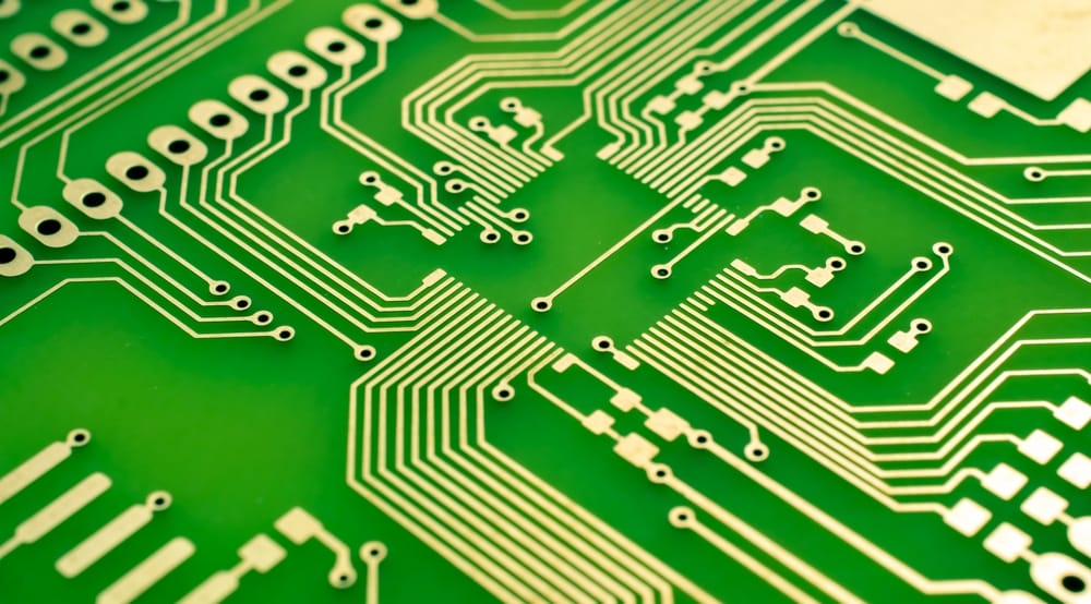
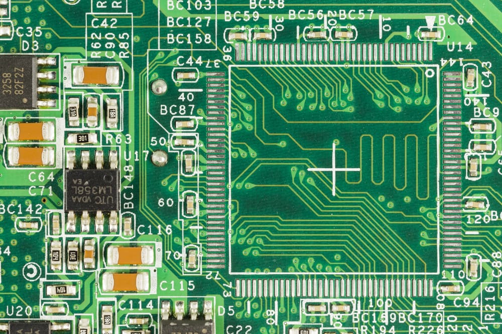
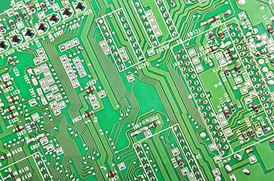
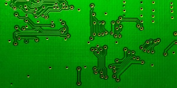
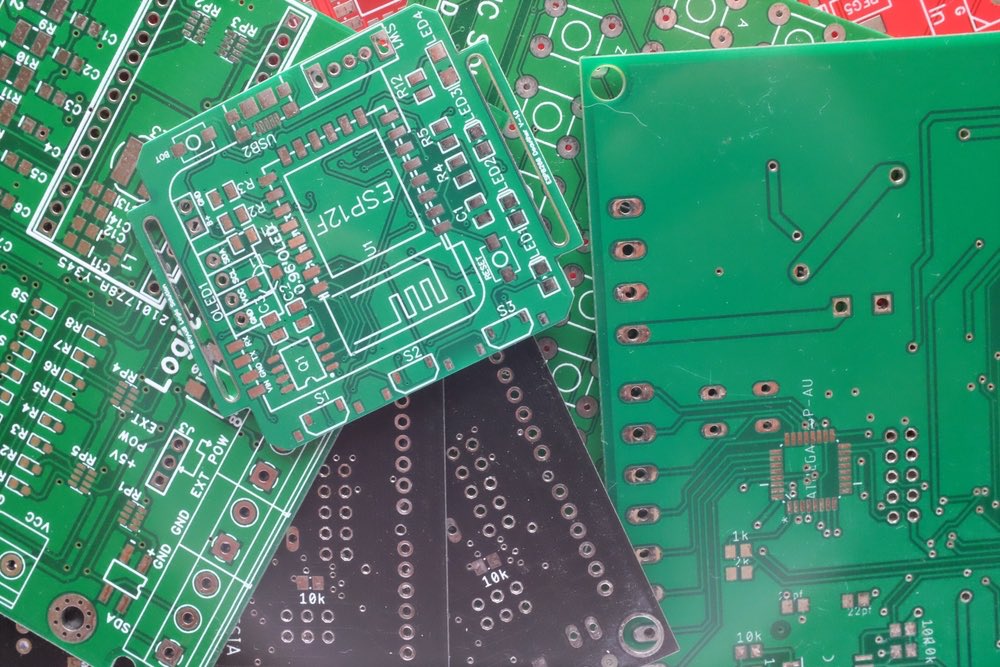
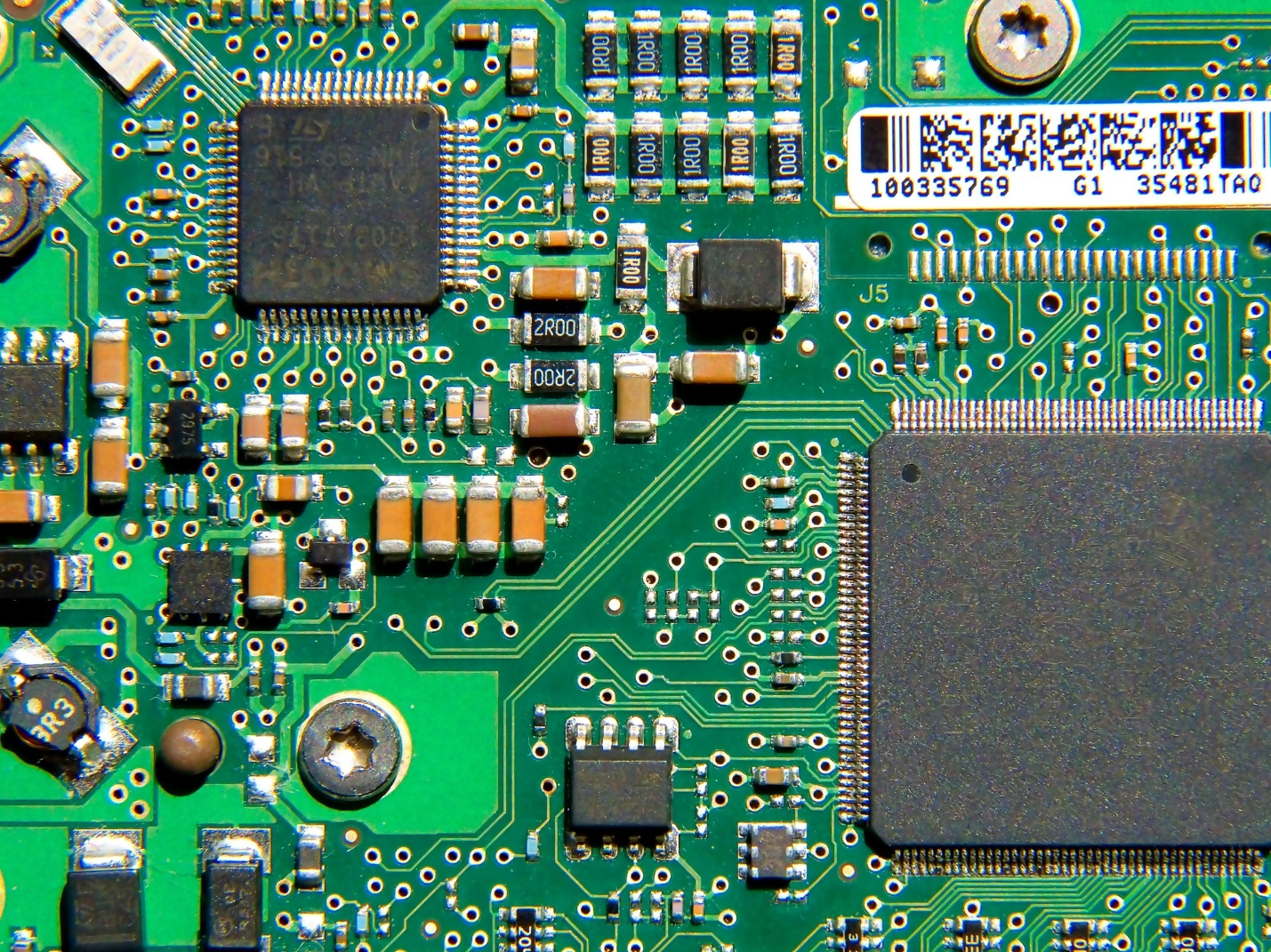
A PCB trace is a highly conductive track that is used to connect components on a printed circuit board. The traces are commonly made of copper and are fabricated during the etching process of a PCB. This article delves into the explanation of PCB trace, its vital components, and its significance to PCB design and fabrication.
Best Guide To PCB Traces: Width, Thickness And Design Fix Recommendations - Jhdpcb
A Detailed Guide on PCB Fabrication Process - The Engineering Projects
How to Design a PCB Layout: A Comprehensive Guide

A detailed guide to PCB layout design - IBE Electronics
Acid Trap PCB Via-Ultimate Guide On All the Things You Need to Know

PCB Layers: Everything You Need to Know
What is a Via: A Comprehensive Guide
Trace PCB: A Comprehensive Guide

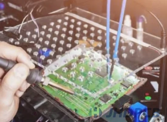
Step-by-Step Guide to Repair PCB Trace - Fx PCB
Recommandé pour vous
 7 Ways to Quickly Judge the Quality of Your Printed Circuit Board14 Jul 2023
 What is PCB Design14 Jul 2023
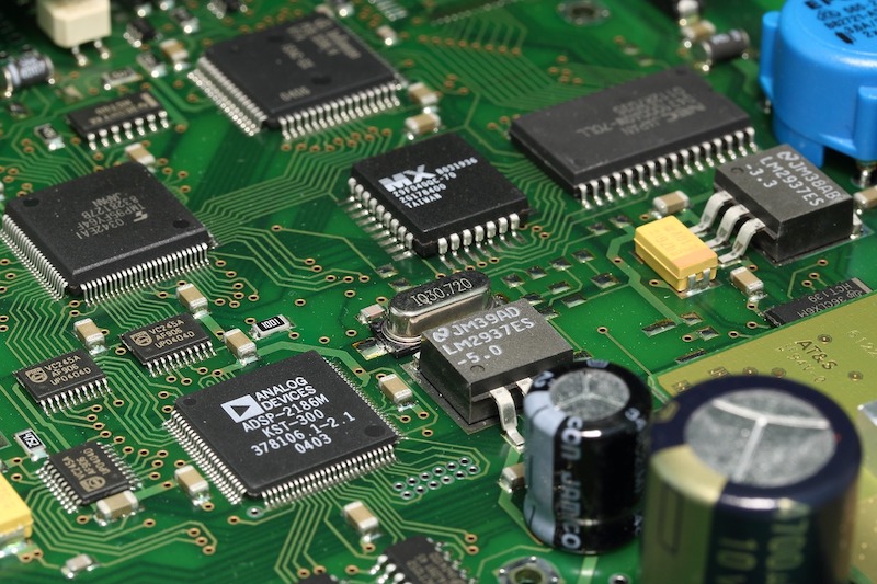 How to Choose a PCB Assembly Company? – Robotics & Automation News14 Jul 2023
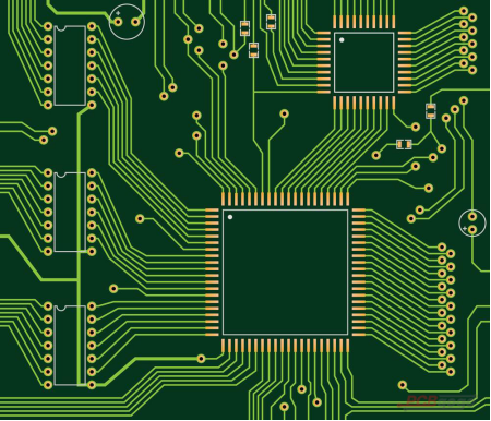 PCB Trace - Everything You Need To Know14 Jul 2023
 High-Volume PCB Assembly is Key to Saving on PCB Design14 Jul 2023
 PCB HS Code Complete Guide - Fx PCB14 Jul 2023
 The 2022 List of Top 10 Printed Circuit Board Manufacturers14 Jul 2023
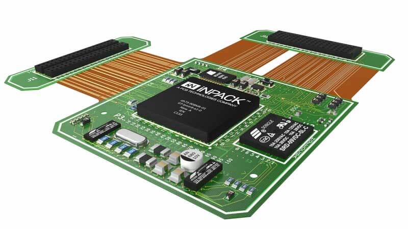 PCB Technologies - PCB Fabrication, PCB Design, IC Packaging14 Jul 2023
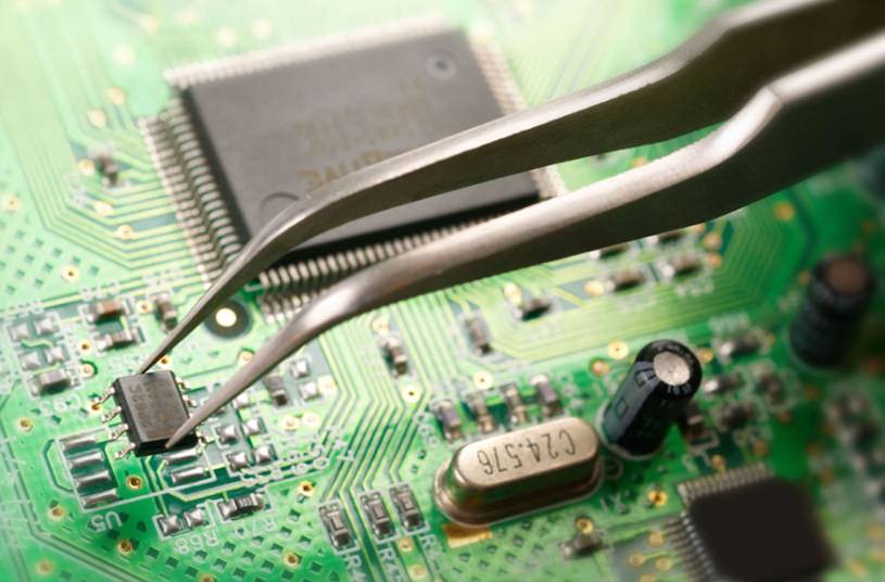 Ultimate Guide to Benchtop PCB Rework & Repair14 Jul 2023
.jpg) 5 things to know about PCB footprints14 Jul 2023
5 things to know about PCB footprints14 Jul 2023
Tu pourrais aussi aimer
 Lampe d'urgence d'extérieur, ampoule Rechargeable, lampe de marché nocturne, charge intelligente, E27, 5W 7W 9W 12W, 220V14 Jul 2023
 Use of eFAST in Patients with Injury to the Thorax or Abdomen14 Jul 2023
 Bouton De Démarrage Et D'arrêt Pour Vw Passat 561959839, 201014 Jul 2023
 Appareil d'entraînement musculaire du plancher pelvien pour femme, exercice de Kegel rotatif, résistant à 360 degrés, antidérapant, réglable pour le corps, les cuisses et les hanches - AliExpress14 Jul 2023
 Hotte aspirante qui fait du bruit : que faire ?14 Jul 2023
 DISNEY PRINCESS Poupée Raiponce14 Jul 2023
 Cale porte HETTICH bois brut beige L.9 x H.2.4 x l.2.9 cm14 Jul 2023
 Biais à quilter thermocollant - Rouleau de 10 mètres - Rouge14 Jul 2023
 Housses Siège Auto Housse Siège Voiture Universelle Pour Elysion Pour Fit Pour Jade Pour Jazz Tous14 Jul 2023
 Barbie Signature Barbie Looks Doll (Curvy, Brunette) – Mattel Creations14 Jul 2023